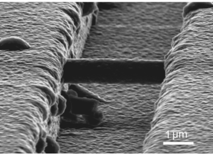
May 20, 2014 – Researchers at UC Davis Center for Nano-MicroManufacturing are experimenting with nanowires and nanostructures to create new electronic circuitry that is not silicon based but can be mated with silicon. The technology exceeds lower threshold limits of silicon chips. It can handle higher voltages and higher temperatures. Applications include sensors, control devices and photonics for automobiles, airplanes, rockets, spacecraft, mining, manufacturing and medical implants.
The nanowire circuitry is made from materials such as gallium arsenide, gallium nitride and indium phosphide which can then be integrated by nanobridges and nanopillars with silicon circuitry. The manufacturing process is similar to current ones used for silicon circuits which makes the technology easy to scale. Because the nanowires are suspended above the circuit boards they can handle heat loads very effectively. At the same time they can be used in transistors that combine materials because the wires do not experience mating issues with a silicon substrate.
Leading the research team is Saif Islam, Professor of Electrical and Computer Engineering. He notes that conventional silicon circuits do not function in temperatures exceeding 250 Celsius (480 Fahrenheit) degrees. But the new technology can. This makes it suitable for industrial applications that silicon circuits could not handle without the additional need for heat ablation adding extra costs. Islam states: “In the foreseeable future, society will be dependent on a variety of sensors and control systems that operate in extreme environments…we can’t grow films of these…materials on silicon, but we can grow them as nanowires.”


